Showing posts with label circuit. Show all posts

Friday, December 12, 2014

6v 12vdc converter circuit

This inverter circuit can provide up to 800mA of 12V power from a 6V supply.
For example, you could run 12V car accessories in a 6V (British?) car.he circuit is simple, about 75% efficient and quite useful. 
By changing just a few components, you can also modify it for different voltages.
Read More..

Friday, November 14, 2014

LIGHT TO FREQUENCY CONVERTER CIRCUIT

This is the circuit diagram of a effective light to frequency converter circuit that can be used for variety of applications such as light intensity measurement,fun etc. This circuit is based on TLC555, the CMOS version of famous timer IC NE 555. A photo diode is used for sensing the light intensity. The timer IC is wired in astable mode. The leakage current of the reverse biased photo diode is proportional to the light intensity falling on it. This leakage current charges the capacitance C1. When the capacitor voltage reaches 2/3 of the supply voltage the out put (pin 3) goes low. As a result the capacitor discharges through photo diode .When the capacitor voltage reaches 1/3 the supply voltage the out put (pin 3) of IC goes high. This cycling continues and we get a frequency at pin 3  proportional to the light intensity falling on the photo diode.

Light to Frequency Converter Circuit Diagram & Parts List


Points to remember

  • With the given components the frequency  varies from 1KHZ @ complete darkness to  24 Khz @  bright sunlight.The frequency range can be changed by using different values for C1.
  • Use any general purpose photo diode for D1.
Read More..

Ultrasonic Mosquito Repeller Circuit Diagram by CD4017

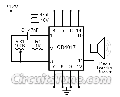
This is a simple ultrasonic mosquito repeller circuit diagram. The circuit is design on the theory that pests like mosquito can be repelled by ultrasonic frequency around (20KHz-25KHz). This ultrasonic mosquito repeller circuit is based on a single CMOS IC CD4017. C1,R1 & VR1 is used to adjust the output frequency.

Circuit Diagram:

Ultrasonic
Fig: Ultrasonic mosquito repeller circuit diagram
Read More..

Wednesday, November 12, 2014

Led light bar scan back and forth led two color circuit with explanation

This circuit is a circuit run on alternating two colors.It uses the 2-color LED with a built-in 3-pin single.This will chase away the glow of each LED until the end.It turns alternating to another color.In any way to the moon on the moon first end, then the LED end of the first LED.Circuit consists of, nand gate ic.Two 10 Counter circuits IC, and IC JK flip flop.

Operation of the circuit is divided into 3 sets.It is a set of signal generators, a set of display and control.Set the signal generator is IC1a,and IC1b number 4011 is a signal generator.The R2, R3, C2 determine the frequency generated.The signal is fed to a set of impressions is the number 4011 IC2 and IC3.The 10 counter circuits to output to the LED, and Is the same, but the work must be performed one at side.

Therefore, the signal from pin 11 of IC 2 and tested for D2 and D3,To pin 3 of IC4.The integrated circuit IC 4 is a JK flip flop is connected to a T flip flop.The signal input pin 3 and pin 1 is the output signal.Which sends a signal to the Reset IC either stop working.IC4 on the anniversary, it will output the first time, in contrast to pin1.IC3 make work, IC2 stopped.
IC2 is controlled by signals from pin 1 of IC4, to IC1c.Prior to control IC2.The IC3 is connected to pins 1 through D1 to the control again.
Read More..

lm3914 led light based music circuit

led

This is a simple light running circuit by music This circuit is not difficult, is MONO, with a few accessories. Can be connected to the output of a CD or cassette player Time.
Operation of the circuit. Begins to be input via VR. The VR will function fine, signal strength coming. D1 will take disconnected hemisphere plus leaving only the signal hemisphere removed to activation of Q1. Signal is extended through Q1 to pin 5 input of IC1. By C1 forward delay of the IC is not the LED (connected to the output. of IC1) off immediately. The IC IC1 is finished. The act shows the effect of the voltage at IC1 pin 5 of the display by the LED to pins 1-19 of the IC, which is within range. compared to a multiple voltage standard circuits. The circuit can operate effectively. In the R1 that it will determine the current flowing through the LED. To prevent LED damage.
Use should be connected to the input of the circuit. To the speaker terminals, change the value of R3 is 10k and IC1 can choose to display two types Bar (Bar) when the pin 9 and a power source. Dots (Dot) on 9-pin to float to drop.

Read More..

Tuesday, November 11, 2014

One second Audible Clock Circuit Schematic

This accurate one-pulse-per-second clock is made with a few common parts and driven from a 50 or 60 Hertz mains supply but with no direct connection to it. A beep or metronome-like click and/or a visible flash, will beat the one-second time and can be useful in many applications in which some sort of time-delay counting in seconds is desirable. The circuit is formed by a CMos 4024 counter/divider chip and 3 diodes, arranged to divide the frequency of the input signal at pin #1 by 50 (or 60, see Notes).

The input impedance at pin #1 is very hight, so simply touching the pin (or a short track or piece of wire connected to it) is usually enough to provide the necessary input signal. Another way to provide an input signal consists in a piece of wire wrapped several times around any convenient mains cable or transformer. No other connection is necessary.

Circuit diagram:


 One second Audible Clock Circuit Diagram

Parts:

R1 = 10K
R2 = 47.K
R3 = 100R
C1 = 1nF-63V
C2 = 10µF-25V
C3 = 100nF-63V
D1 = 1N4148
D2 = 1N4148
D3 = 1N4148
D4 = LED-(Optional, any shape and color, see Notes)
D5 = 1N4148-75V 150mA Diode (Optional, see Notes)
Q1 = BC337-45V 800mA NPN Transistor
IC1 = 4024-7 stage ripple counter IC
BZ1 = Piezo sounder (incorporating 3KHz oscillator)
SPKR = 8 Ohm, 40 - 50mm diameter Loudspeaker (Optional, see Notes)
SW1 = SPST Toggle or Slide Switch (Optional, see Notes)
B1 = 3 to 12V Battery (See Notes)

Notes:

  • To allow precise circuit operation in places where the mains supply frequency is rated at 60Hz, the circuit must be modified as follows: disconnect the Cathode of D1 from pin #11 of IC1 and connect it to pin #9. Add a further 1N4148 diode, connecting its Anode to R1 and the Cathode to pin #6 of IC1: thats all!
  • The circuit will work fine with battery voltages in the 3 -12V range.
  • The visual display, formed by D4 and R3 is optional. Please note that R3 value shown in the Parts list is suited to low battery voltages. If 9V or higher voltages are used, change its value to 1K.
  • If a metronome-like click is needed, R2 and BZ1 must be omitted and substituted by the circuit shown enclosed in dashed lines, right-side of the diagram.
  • Stand-by current drawing is negligible, so SW1 can be omitted.
Read More..

Friday, November 7, 2014

6Volt Doorbell Light Circuit

This 6V battery operated doorbell light circuit can be affiliated in alongside with any absolute AC230V doorbell. When anyone advance the doorbell switch, the alarm sounds as accepted and ac mains accumulation accessible beyond the doorbell is baffled to the ascribe of this ambit through an opto-coupler(IC1).


Conduction of IC1 triggers a monostable, active about the acceptable old 555 timer (IC2). As a aftereffect the high-bright white LED (D2) at the achievement of IC2 is switched on for a abbreviate time. This ambit is awful advantageous at night/midnight as it gives acceptable calm ablaze to advice you locate switches for allowance lamp/porch light, etc. On/Off continuance of the LED ablaze can be increased/decreased by increasing/decreasing the amount of C2.
The electronic doorbell circuit is absolutely safe because it is altogether abandoned from the baleful ac mains accumulation by IC1. However, accumulate to abstain adventitious contacts with the foreground end of the circuit, which is anon affiliated to the ac supply. Use of a acceptable and acceptable ABS asylum is recommended for this doorbell ablaze unit. 
Read More..

9 Volt 2 Ampere DC Power Supply Circuit Diagram

There is little to be said about this circuit. All the work is done by the regulator. The 7809 can deliver up to 2 amps continuous output whilst maintaining a low noise and very well regulated supply. The circuit will work without the extra components, but for reverse polarity protection a 1N5400 diode (D1) is provided at the input, extra smoothing being provided by C1. The output stage includes C2 for extra filtering, if powering a logic circuit than a 100nF (C3) capacitor is also desirable to remove any high frequency switching noise.Circuit diagram:

Parts:C1 = 100uF-25V electrolytic capacitor, at least 25V voltage rating
C2 = 10uF-25V electrolytic capacitor, at least 6-16V voltage rating
C3 = 100nF-63V ceramic or polyester capacitor
IC = 7809 Positive Voltage Regulator IC
D1 = 1N5400 Diode
Read More..

Thursday, November 6, 2014

Converter Circuit 240V AC TO 5VDC POWER SUPPLY used 7805 Regulator

Converter Circuit 240V AC TO 5VDC POWER SUPPLY used 7805 Regulator
This is simple way to power some 5v logic from a 240v ac source. If a 120v ac power adapter is used, the circuit will also work for 120v ac power lines.
Read More..

Monday, November 3, 2014

stk392 datasheet schematic circuit diagram

The STK392-020 is a hybrid IC for video projector
convergence correction. Since this IC integrates three
output amplifier circuits in a single package, the six
convergence correction output circuits, i.e., the vertical
and horizontal directions for each CRT of the RGB can be
formed from only two ICs.

Applications
Video projectors (both standard and high definition)                                            test circuit
                                                                                             
Features
•Three output amplifier circuits integrated in a single
22-pin package
•High absolute maximum supply voltage
(VCC max = ±44 V)
•Low thermal resistance (θj-c = 2.1 °C/W)
•High thermal stability (TC max = 125°C)
•Isolated early stage and output stage power supplies
•Output stage power supply switching supports high
efficiency designs.

•The input system, power supply system and output
system pins are isolated in the pin arrangement, thus
reducing the influence of the pattern layout on the
characteristics and easing design.
•Since constant current circuits are used in the pre-driver
stage, operation is stable with respect to the power
supply switching.
•The Sanyo convergence correction circuit product
lineup (the STK392-000 series) handles a wide range of
end-product classes. Therefore, the same PCB can be
used for end products from popularly-priced units to
top-of-the-line models. Package Dimensions
Read More..

100W Audio Amplifier Transistor used BDW83D BDW84D circuit diagram

Here 100 watt power audio amplifier which using power transistor BDW83D and BDW84D. Copyright belong to Smart Kit. Schematic diagram:

Component part list:

R1 = 1,2 K                                   D1 = 1N4002-7  
R2 = 0,47 OHM                           D2 = 1N2002-7  
R3 = 220 OHM                            D3 =  1N4148     
R4 = 3,9 K                                   D4 = 1N4148      
R5 = 2,2 K                                   D5 = 1N4148      
R6 = 2,2 K                                    D7 = 1N4148     
R7 = 10 K                                    D8 = 1N4148      
R8  = 4,7 K                                  Q1 = BDW84D   
R9 = 150 OHM                            Q2 = BD829       
R10 = 39 OHM                            Q3 = BC546       
R11 = 3,3 K                                  Q4 = BC556      

Read More..

Saturday, November 1, 2014

Very Simple Audio Mixer Circuit

A very simple audio mixer can be designed using this circuit diagram electronic project. Audio mixing is normally performed by a mixer with virtual ground, in which the various input signals are applied through series resistors to virtual ground, that at the inverting input of operational amplifier. 

Very

The audio mixer is a little different and uses the principle of common ground, the input voltages are converted into alternating current which, when summed, is the AC component of the collector. In the case of a common base configuration, emitter impedance is small and works as a virtual ground that is making it impossible to crosstalk between different input signals. The output signal is taken from the collector of Q1. Amplification circuit is equal to R6 + Ri, where Ri is the input resistance (= one of the resistances RI ... R5). The T1s emitter circuit has been provided a power source consisting of T2 and T3.

Q1s base voltage is set by resistors R7 and R8. Ensure that the capacitor C1 of T1 to be effectively disconnected.
Number of entries can be modified, increased or decreased as desired.
Read More..

Friday, October 31, 2014

OCL Power Amplifier Circuit MJ15003 MJ15004

This Power Amp OCL 100 watt circuit by transistors.They has been an old circuits, but very well amplifier schematic. We use only all transistor MJ15003 and MJ15004 is the main in circuits, and the power supply +38V 0 -38V 3A. follow stye of OCL amp and They has Specification are
power output : 105watt at 4 ohm load, 88watt at 8 ohms load
input sensitivity : 0.5V
Frequency response : 10-10kHZ +/- 1dB
THD: 0.07% at 50 watt , 0.1% at 100 watt.

This power amp OCL 100w is a very excellent sound quality. Since we provide the circuit in look All direct coupling form is connection join together direct all, to cut-off frequency low-loss problems, the super bass really do not tell who.
The signal Input of the tone controls enter via C1 to the base pin of transistor Q1, which together with the Q2 is differential amplifier, the signal from the collection pin of Q1 supplied to the bas pin of the Q5, which it acts as the pre-driver circuit.
- The transistor Q4 is setting level bias or act as to control Idle current in this circuit. Which we can adjust level idle current by By adjusting the VR1.
- The transistor Q3 acts as a boost trapping.
- The output signal from the Q5 will enter to base pin of Q8,Q9.which acts as the driver circuit. For the signal output to drive the output transistors Q10, Q11.
- Both output transistors Q10, Q11, we used the number on the circuit are MJ15003, MJ15004. This couple can use up to 200W, so not problem in durability.
If you want to save. May be represented by a pair of output are 2N3055, MJ2955 each of the two parallel each other instead.

OCL
100W OCL Power Amplifier Circuit MJ15003,MJ15004

Creation
-Check the assembly of all equipment to correct the circuit, without the output transistors, Using a voltmeter measure the voltage at the speaker. By also does not have a speaker. At the end of this process was completed and ready to operate immediately.
-Put the power supply to the circuit, then to measure the voltage is 0V or not higher than 0.25V, if not in this means that the circuit failure, need to check first.
-The later, on output transistors, and then use an ammeter to measure the current is supplied with short input circuit. Measuring that positive or negative wire. Then, adjust VR1 until reading about the current 20-40 mA.
- For transistor Q4, when the device successfully. Should be installed on the cooling pad. Which installation of the output transistor. To help control the the bias current output relative to the temperature change of the output transistor.
- The power supply circuit is got by power of transformer T1, which provides voltage to the coil in the secondary coil is 27-0-27 volt, 5 amp.
- The Diodes Bridge rectifier should be not lower than 5 Amp 100V, The filter capacitor C7, C8 we used a 1,000uF 50V, the voltage at the capacitor afer through the filter will can about 38V.
Read More..

Master Slave Switch Circuit

In this age of enlightenment any sort of relationship that could be described as master/slave would be questionable but for the purposes of this circuit it gives a good idea of how it functions. The circuit senses mains current supplied to a ‘master’ device and switches ‘slave’ equipment on or off. This feature is useful in a typical hi-fi or home computer environment where several peripheral devices can all be switched on or off together. A solid-state relay from Sharp is an ideal switching element in this application; a built-in zero crossing detector ensures that switching only occurs when the mains voltage passes through zero and any resultant interference is kept to an absolute minimum.

master-slave-switch-circuit-diagramw

Master/Slave Switch Circuit Diagram

All of the triac drive circuitry (including optical coupling) is integrated on-chip so there are very few external components and no additional power supply necessary. This makes the finished design very compact. Diodes D1, D2, D3 and D4 perform the current sensing function and produce a voltage on C2 when the master equipment is switched on. A Schottky diode is used for D5 to reduce forward voltage losses to a minimum. The circuit is quite sensitive and will successfully switch the slave even when the master equipment draws very little mains current. The RC network formed by R1 and C1 provides some protection for the solid-state relay against mains-borne voltage transients.

Warning:

This circuit is connected to the mains. it is important to be aware that the chip has lethal voltages on its pins and all appropriate safety guidelines must be adhered to! This includes the LED, for safety it must be fitted behind a transparent plexiglass shield.

Author: Karl Köckeis - Copyright: Elektor July-August 200

Source : www.extremecircuits.net

Read More..

Thursday, October 30, 2014

Circuit 150W amplifier with active crossover

stereo
Series 150W Amplifier With Active Crossover Series 150W Amplifier with Active Crossover is very interesting. Actually, this circuit uses 4-channel power amplifier chip. Well, as an Active Crossover here we use also a chip that can separate the tone of the bass, midrange and treble, the output from the Active Crossover can be directly amplified by power amplifier.

Power Chip 4-channel amplifier that we use is SANYO LA47536 who have power outputs up to 150W, while for Active Crossover (Active Crossover) we use the LF353 from National Semiconductor.

stereo
Read More..

UM3561 Heat detector alarm circuit with explanation

 um3561 heat detector alarm circuit with explanation
A very simple heat detector alarm electronic project can be designed using the UM3561 sound generator circuit and some other common electronic parts . This heat detector electronic circuit project uses a complementary pair comprising npn and pnp transistor to detect heat . Collector of T1 transistor is connected to the base of the T2 transistor , while the collector of T2 transistor is connected to RL1 relay . T3 and T4 transistors connected in darlington configuration are used to amplify the audio signal from the UM3561 ic .
When the temperature close to the T1 transistor is hot , the resistance to the emitter –collector goes low and it starts conducting . In same time T2 transistor conducts , because its base is connected to the collector of T1 transistor and the RL1 relay energized and switches on the siren which produce a fire engine alarm sound .
This electronic circuit project must be powered from a 6 volts DC power supply , but the UM3561 IC is powered using a 3 volt zener diode , because the alarm sound require a 3 volts dc power supply .
The relay used in this project must be a 6 volt / 100 ohms relay and the speaker must have a 8 ohms load and 1 watt power
Read More..

Wednesday, October 29, 2014

LM1875 20W audio amplifier Diagram Circuit

Description.
This is just another 20W audio amplifier circuit , but this time based on the LM1875 audio amplifier IC from National Semiconductors. With a 25V dual power supply LM1875 can deliver 20W of audio power into a 4 ohm speaker. The LM1875 requires very less external components and has very low distortion. The IC is also packed with a lot good features like fast slew rate, wide supply voltage range, high output current, high output voltage swing, thermal protection etc. The IC is available in TO-220 plastic power package and is well suitable for a variety of applications like audio systems, servo amplifiers, home theatre systems etc.
Circuit diagram.

Notes.
 lm1875 20w audio amplifier circuit and explanation
  • Assemble the circuit on a good quality PCB.
  • Use +/-25V DC dual supply for powering the circuit.
  • K1 can be 4 ohm, 20W speaker.
  • A proper heat sink is necessary for the IC.
  • F1 and F2 are 2A fuses.
Read More..

USB Powered Audio Power Amplifier Circuit Diagram

This is the simple USB Powered Audio Power Amplifier Circuit Diagram. This circuit of multimedia speakers for PCs has single-chip-based design, low-voltage power supply, compatibility with USB power, easy heat-sinking, low cost, high flexibility and wide temperature tolerance. At the heart of the circuit is IC TDA2822M. This IC is, in fact, mono-lithic type in 8-lead mini DIP package. It is intended for use as a dual audio power amplifier in battery-powered sound players. Specifications of TDA2822M are low quiescent current, low crossover distortion, supply voltage down to 1.8 volts and minimum output power of around 450 mW/channel with 4-ohm loudspeaker at 5V DC supply input. 

An ideal power amplifier can be simply defined as a circuit that can deliver audio power into external loads without generating significant signal distortion and without consuming excessive quiescent current. This circuit is powered by 5V DC supply available from the USB port of the PC. When power switch S1 is flipped to ‘on’ position, 5V power supply is extended to the circuit and power-indicator red LED1 lights up instantly. Resistor R1 is a current surge limiter and capacitors C1 and C4 act as buffers. Working of the circuit is simple. Audio signals from the PC audio socket/headphone socket are fed to the amplifier circuit through components R2 and C2 (left channel), and R3 and C3 (right channel).

Circuit diagram:


USB Powered Audio Power Amplifier Circuit Diagram

Potmeter VR1 works as the volume controller for left (L) channel and potmeter VR2 works for right (R) channel. Pin 7 of TDA2822M receives the left-channel sound signals and pin 6 receives the right-channel signals through VR1 and VR2, respectively. Ampl i f ied signals for driving the left and right loudspeakers are available at pins 1 and 3 of IC1, respectively. Components R5 and C8, and R6 and C10 form the traditional zobel network. Assemble the circuit on a medium-size, general-purpose PCB and enclose in a suitable cabinet. It is advisable to use a socket for IC TDA2822M. The external connections should be made using suitably screened wires for better result.


Sourced By: EFY
Read More..

Tuesday, October 28, 2014

Automatic Emergency Lamp Circuit

This is an automatic emergency lamp with day light sensing, means it senses darkness/night and turns ON automatically. Similarly it senses day light and turns OFF automatically. A simple emergency lamp which does not require any special equipment; even a multimeter to assemble and use. Any individual who can do a good quality soldering must be able to build this circuit successfully.

This can be easily accommodated in the defunct two 6 watt tube National Emergency Lamp or any PL tube type emergency lamp. The difference will be in the working; it will work non stop for more than 8 hours. Deep discharge is taken care by the LED characteristic and over charge protection is taken care by the fixed voltage regulator.This uses a simple 3Pin fixed regulator which has a built in current limiting circuit.

Simple Emergency Light Circuit Diagram: 

Automatic
Automatic Emergency Lamp Circuit
The only required adjustment is the preset which has to be set to ensure the LEDs just light up (it should be left at that position). The 5mm LDR is just mounted on top of the emergency light as shown in the photograph. LDR is used to avoid it lighting up during day time or when the room lights are ON. 2 LEDs are used in series; the dropping resistance is avoided and 2 LEDs light up with current that is required for a single LED,  by which energy is saved to a great extent.

This particular circuit has been kept so simple for people who has limited access to components or in other words this is an emergency light that you can build with minimum components. In addition to circuit diagram, He has shared photographs of the prototype he made in National emergency light and a PCB design.
Read More..

Monday, October 27, 2014

300W Power Amplifier Circuit with 2N773

Power Amplifier 300W with transistor 2N3773
This amplifier was designed to provide a use for the otherwise useless TO3 power transistors that many hobbyists have in their junk pile.  With good construction the module is capable of high quality performance and is rated to 300 watts into a 4 ohm load depending on power supply.  With the driver and output transistors specified it is limited to DC rails of +/- 70 volts. 

Power Amplifier Circuit Diagram

Read More..