Showing posts with label v. Show all posts

Tuesday, August 26, 2014

Simple F and V Converter Wiring diagram Schematic

This is a best Frequency/Voltage Converter schema diagram proportional voltage by the use of a frequency-to-voltage (F/V) converter. Teledyne Semiconductor`s Type TSC9402 is a versatile IC. Not only can it convert voltage into frequency, but also frequency into voltage. It is thus eminently suitable for use in an add-on unit for measuring frequencies with a multimeter. 

 Best F and V Converter Circuit Diagram


Best


Only a few additional components are required for this.. Just one calibration point sets the center of the measuring range (or of that part of the range that is used most frequently). The frequency-proportional direct voltage at the output (pin 12—amp out) contains interference pulses at levels up to 0.7 V. If these have an adverse effect on the multimeter, they can be suppressed with the aid of a simple RC network. 

The output voltage, U0, is calculated by: tfo=C/rei(Ci + 12 pF) R2fm Because the internal capacitance often has a greater value than the 12 pF taken here, the formula does not yield an absolute value. The schema has a frequency range of dc to 10 kHz. At 10 kHz, the formula gives a value of 3.4 V. The schema draws a current of not more than 1 mA. 

Sourced By : Circuitsstream
Read More..

Sunday, August 24, 2014

LED at 230 V

Small schema to run a LED on line voltage (English)

This little schema allows to connect a LED to line voltage. A LED can not handle with 230V AC and needs a current which is limted to ca. 15mA. The first issue is simply solved with a diode which eliminates the voltage in reverse-biasing. The current is limited by the combination of the resistor and capacitor. Used at AC capacitors work as frequency dependent resistors. You can simply calculate the capacitive resistance of the capacitor by the following formula:
Formula
Based on a frequency of 50Hz and a capacity of 220nF you get a reactance of ca. 16kΩ. This is just perfect for a LED. The resistor prevents that the capacitor does not charge that abruptly.

Hinweis

Attention. This schema works with life threatening line voltage. All parts of this schema are connected to the grid! You have to make sure that it is not possible to touch any parts of the schema at any time. You have to unplug the schema everytime you want to check it.

Part list

  • C1: foil capacitor 220nF, 250V~ (stick to the values!)
  • R1: 2,2kΩ
  • R2: 220Ω
  • D1: 1N4007 (or comparable; must be suitable for 220V/230V)
  • LED1: standard LED

Circuit diagram

Circuit


Source by : Benedikt Wirmer

Read More..

Tuesday, August 12, 2014

12 V AC Dimmer

12-V AC Dimmer Circuit Diagram The schema described here is derived from a conventional design for a simple lamp dimmer, as you can see if you imagine a diac connected between points A and B. The difference between this schema and a normal diac schema is that a diac schema won’t work at 12 V. This is the fault of the diac. Most diacs have a trigger voltage in the range of 30 to 40V, so they can’t work at 12 V, which means the dimmer also can’t work.


12-V AC Dimmer Circuit Diagram

The portion of the schema between points A and B acts like a diac with a trigger voltage of approximately 5.5 V. The network formed by R1, P1 and C1 generates a phase shift relative to the supply voltage. The ‘diac equivalent’ schema outputs a phase-shifted trigger pulse to the triac on each positive and negative half-cycle of the sinusoidal AC voltage.

This works as follows. First consider the positive half of the sine wave. C1 charges when the voltage starts to rise, with a time constant determined by C1, R1 and P1. T1 does not start conducting right away. It waits until the voltage across D2 reaches 4.7 V and the Zener diode starts to conduct. Then current starts to flow, driving T1 and T3 into conduction. This produces a pulse at point B. The same principle applies to the negative half of the sine wave, in this case with D1, T2 and T4 as the key players.

The trigger angle can be adjusted with P1 over a range of approximately 15 degrees to 90 degrees. C2 provides a certain amount of noise decoupling. Depending on the load, the triac may need a heat sink. You can use practically any desired transistors; the types indicated here are only examples. If the schema does not dim far enough, you can change the value of P1 to 25 kΩ. This allows the trigger angle to be increased to 135 degrees.

Note: this schema works fine with normal transformers, but not with ‘electronic ’ transformers.

Read More..

Sunday, August 10, 2014

V Charger Wiring diagram Schematic

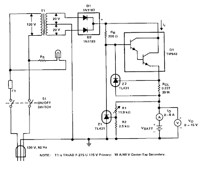
The charger is based on a charging voltage of 2.4 V per cell, in accordance with most manufacturers recommendations. The schema pulses the battery under charge with 14.4 V (6 cells ? 2.4 V per cell) at a rate of 120 Hz. The design provides current limiting to protect the chargers internal components while limiting the charging rate to prevent damaging severely discharged lead-acid batteries. 

The maximum recommended charging current is normally about one-fourth the ampere-hour rating of the battery. For example, the maximum charging current for an average 44 ampere-hour battery is 11 A. If the impedance of the load requires a charging current greater than the 11 A current limit, the schema will go into current limiting. The amplitude of the charging pulses is controlled to maintain a maximum peak charging current of 11 A (8 A average).

V Charger Circuit Diagram

V Charger Circuit Diagram

V Charger Circuit Diagram
Read More..